#lithography

berternste2@diasp.nl

De aardappeleters

Foto van een steen voor het reproduceren van tekeningen (lithografie), in dit geval van De Aardappeleters van van Gogh

Woerden (Utrecht) 2018

Een steen voor het afdrukken van een tekening van De Aardappeleters van Vincent van Gogh. Van Gogh ging niet helemaal volgens het boekje te werk bij het maken van de litho volgens de tekst bij deze steen in het Woerdense Stadsmuseum:

Foto van het tekstbord bij de litho

#art #foto #fotografie #jaarbeurs #kunst #litho #lithography #litografie #netherlands #photo #photography #steendruk #van-gogh #woerden

Originally posted at: https://blog.ernste.net/2024/09/15/de-aardappeleters/

jakob@pod.orkz.net

James Rattray

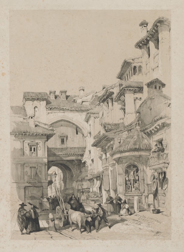
Temple of 'Ahmed Shauh', King of Afghanistan

The current situation in Afghanistan in desperate. Posting memes found on Twitter doesn't mean anything and won't change a thing. Nothing will. But I do think about it and then I just have to go into the escapist dream world of history.

This is how the tomb of the King Aḥmad Shāh Durrānī (I know, a tautology, as shah already means king) who conquered Delhi and more or less founded modern Afghanistan, looked in 1848. The building is still there in Kandahar. James Rattray was a British Lieutenant who made a rather fascinating work with a lot of ethnographic lithographies from his own sketches. I have been looking at other pictures to see those stately mountains and even though it might be exaggerated in this it does seem that it is a beautiful city in the mountains.

#art #print #lithography #graphicprint #graphicart #JamesRattray #AhmadShah #tomb #Kandahar #Afghanistan #1848

waynerad@pluspora.com

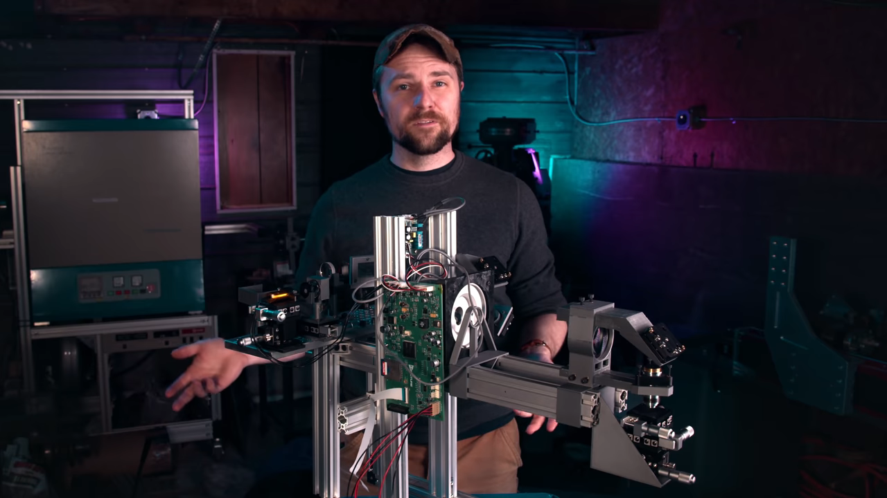
What ASML has next after EUV. ASML ("Advanced Semiconductor Materials Lithography") being the world's biggest chip manufacturing equipment provider, and EUV being "extreme ultraviolet" -- lithography using extremely short wavelengths of light. ASML already has basic EUV systems working, and companies are using them to manufacture chips. What's next?

It's all about the NA. "NA" stands for numerical aperture. The "numerical aperature" tells you the range of angles over which a lens or other optical system can emit or receive light. He illustrates this with "light cones" in the video which visually illustrates from which angles light can strike the surface of the semiconductor. The larger the NA, the larger the range of angles.

He uses the term "pitch" without defining it. In semiconductor lithography, the "half pitch" is generally the smallest feature size that can be etched on the chip. If you wanted two wires next to each other, you'd need a half pitch for each wire width and another half pitch for the gab between them. Therefore the distance from the edge of one wire to the corresponding edge of the wire next to it would be two half pitches -- in other words, a full pitch. So "pitch" refers to the distance between two wires on the chip.

What ASML has next after EUV

#solidstatelife #lithography #euv #asml