#asml

Twinscan Exe 5000: ASML bringt Lego-Modell einer Prozessorfertigungsmaschine - Golem.de
@carstenraddatz_fca@nerdica.net Ist ja bald Weihnachten ;)
#asml
One person like that
1 Comments
1 Shares
U onderschat de fatale gevolgen van een Russische overwinning
NRC
Oorlog - Belanden we straks in de Derde Wereldoorlog omdat de Tweede te lang geleden en daardoor ‘vergeten’ is? Europa is niet voorbereid op het feit dat Poetin zich niet laat tegenhouden door gebaren van onze goede wil, en de burger gedraagt zich als een passieve consument, aldus Thomas von der Dunk.
(Tekst loopt door onder de foto.)
:format(webp)/s3/static.nrc.nl/bvhw/files/2024/02/data111404755-0ebd47.jpg)
De Russische president Vladimir Poetin begin dit jaar, gezien door het licht van een tv-camera. Foto Maxim Shemetov/Reuters.
Nooit eerder in de afgelopen halve eeuw is het gevaar van een nieuwe wereldoorlog zo groot geweest. En nooit eerder heeft het Westen er zo beroerd voor gestaan. Het huidige Rusland vormt een veel grotere bedreiging dan de Sovjet-Unie tijdens Chroestjov of Brezjnev ooit is geweest. (...)
Daarbij heeft [Poetin] zijn kaarten op de interne verdeeldheid van het Westen gezet. Ook in dat opzicht staat het er beroerder voor dan ooit. De Verenigde Staten zijn inmiddels een verscheurde natie; een herverkiezing van Trump zal Amerika een isolationistische koers doen inslaan. Europa is intern eveneens ernstig verzwakt, nu in veel landen een kwart van het electoraat op semi-fascistische partijen stemt die begrip of zelfs sympathie voor Poetin tonen, ook in Nederland. (...)
En dan het derde rampzalige grote verschil. Nikolaos van Dam heeft in NRC (23/1) terecht met de misdadige stupiditeit van het Nederlandse Israëlbeleid de vloer aangeveegd. Met het wegkijken bij de massale schending van het oorlogsrecht door Netanyahu ondermijnt het Westen zelf de internationale rechtsorde die het tegenover Rusland beweert te verdedigen. (...)
Dat betekent: intern en extern sterk verzwakt, staat Europa er alleen voor. De urgentie is groot –- niet toevallig luidde een reeks van hoge Europese militairen recent de noodklok -–maar die urgentie wordt onvoldoende beseft. (...)
In de Europese samenleving is nog veel te weinig het besef ingedaald dat Poetins oorlog ook de ‘onze’ is, reeds omdat Poetin zelf die als zodanig beschouwt. Daarvoor kijkt men weg. Het is daarbij symptomatisch dat tijdens de verkiezingscampagne het buitenland totaal niet aan bod kwam. (...)
Vandaar de aarzeling om zware wapens te leveren, uit angst voor escalatie – in de hoop hiermee Poetin ook tot matiging te bewegen. Dit werkt alleen averechts. (...)
Europa blijkt vervolgens niet voorbereid op het feit dat Poetin zich niet laat tegenhouden door gebaren van onze goede wil. (...) Daarin schuilt de parallel met de Tweede Wereldoorlog, waarop men niet meer alert is: een zelfde aarzeling, om maar vooral niet Poetin te provoceren, die toen bij Hitler bestond. (...)
Daarbij heeft dertig jaar neoliberalisme de kiezer van een actieve burger in een passieve consument veranderd, wiens collectieve verantwoordelijkheidsbesef is afgenomen, omdat voor de strontverwende middenklasse de onmiddellijke bevrediging van elke behoefte aan luxeproducten een grondrecht geworden is. (...) Een politicus die dan de productie van tanks ten koste van tv’s durft te laten gaan, krijgt het electoraal moeilijk. Een consument brengt pas offers als het echt onontkoombaar is, en in een oorlogssituatie is het dan te laat.
Dat twee jaar na 24 februari 2022 Europese regeringen nog steeds niet fabrieken gewoon tot omschakeling op militaire productie kunnen en durven dwingen, hangt daarmee rechtstreeks samen. (...)
> Zie ook: Poetins lange oorlog
Tags: #nederlands #oorlog #poetin #putin #rusland #oekraine #ukraine #europa #eu #europese_unie #wapens #zware_wapens #trump #internationale_rechtsorde #oorlogseconomie #asml
/s3/static.nrc.nl/bvhw/files/2024/02/data111404755-0ebd47.jpg)
5 Likes
1 Comments
Japan and the Netherlands agreed "to tighten restrictions on the export of chip manufacturing technology to Chinese companies."
"ASML is the most critical company affected by the Netherlands' restrictions. It's the only company in the world that produces so-called ultraviolet lithography machines, which are critical to the production of advanced semiconductors. CNBC previously reported that the company was already unable to ship its advanced extreme ultraviolet lithography (EUV) machine to China but that it could still ship older deep ultraviolet lithography (DUV) machines."
"On the Japanese side, the restrictions are expected to impact companies such as Nikon and Tokyo Electron."
Japan and the Netherlands join US with tough chip controls on China
#solidstatelife #semiconductors #euv #asml #exportrestrictions #geopolitics
/cdn.vox-cdn.com/uploads/chorus_asset/file/24389544/1242819188.jpg)
One person like that
1 Shares
Ik doe normaal niet aan complottheorieën, maar nu ben ik toch echt iets op het spoor
Jamal Ouariachi (Trouw)
(...) De Amerikanen slaan nogal eens de plank mis met hun buitenlandpolitiek, maar nu niet: Nederlandse chipfabrikanten stinken een beetje. NOS en Nieuwsuur onthulden vorige week dat er miljoenen Nederlandse chips in Rusland belanden, via China. Zo werden recentelijk op het slagveld in Oekraïne microchips van het Eindhovense NXP aangetroffen in een uit elkaar gehaalde Russische pantserhouwitser, een kruisraket en een gevechtshelikopter. In Russische drones zijn chips van het Nijmeegse Nexperia gevonden. (...)
(Tekst loopt door onder de foto.)
Jamal Ouariachi

Gelukkig hebben we de Russen niet nodig voor een gifwolk boven Nederland. Met dank aan Schiphol. Voor 99,9 procent van de uitstoot van schadelijke stoffen op de luchthaven gelden geen regels. (...)
Toch is volgens Rutte hét grote gevaar voor Nederland de ‘linkse wolk’. Dat beweerde de premier althans in een interview met De Telegraaf, samen met Eerste Kamer-lijsttrekker voor de VVD Edith Schippers. Wie? Edith Schippers, die in haar tijd als minister van volksgezondheid nauwe banden onderhield met de tabaksindustrie en een Big Brother Award kreeg uitgereikt. Edith Schippers, wier man grof geld verdiende met het adviseren van zorginstellingen over de wetgeving van zijn vrouw. Edith Schippers, onder wier bestuursvoorzitterschap van pensioenfonds DSM 900 miljoen euro bedoeld voor pensioengerechtigden in rook – ik bedoel: een VVD-wolk – opging. (...)
Ik doe normaal niet aan complottheorieën, maar nu ben ik toch echt iets op het spoor. Nederlandse microchips in Russisch wapentuig, gifgassen van Schiphol, een pensioensloper als Eerste Kamer-lijsttrekker: een suïcidale VVD-wolk is erop uit Nederland kapot te maken.
Tags: #nederlands #nederland #rutte #mark_rutte #vvd #chipfabrikanten #nxp #nexperia #asml #rusland #oekraine #wapenexport #schiphol #luchtvervuiling #schadelijke_stoffen #lobby #tabakslobby #schippers #edith_schippers #pensioenfonds #dsm #zorg #volksgezondheid #zorginstelling

2 Likes
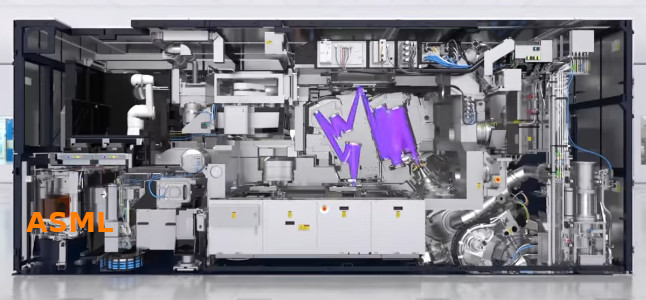
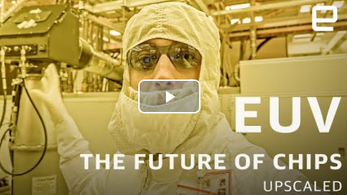
What ASML has next after EUV. ASML ("Advanced Semiconductor Materials Lithography") being the world's biggest chip manufacturing equipment provider, and EUV being "extreme ultraviolet" -- lithography using extremely short wavelengths of light. ASML already has basic EUV systems working, and companies are using them to manufacture chips. What's next?
It's all about the NA. "NA" stands for numerical aperture. The "numerical aperature" tells you the range of angles over which a lens or other optical system can emit or receive light. He illustrates this with "light cones" in the video which visually illustrates from which angles light can strike the surface of the semiconductor. The larger the NA, the larger the range of angles.
He uses the term "pitch" without defining it. In semiconductor lithography, the "half pitch" is generally the smallest feature size that can be etched on the chip. If you wanted two wires next to each other, you'd need a half pitch for each wire width and another half pitch for the gab between them. Therefore the distance from the edge of one wire to the corresponding edge of the wire next to it would be two half pitches -- in other words, a full pitch. So "pitch" refers to the distance between two wires on the chip.
#solidstatelife #lithography #euv #asml
2 Likes
1 Comments
1 Shares
fascinating video(s)
thanks for making & sharing 🙂 will do the best to assemble an informative article 🙂
https://ytpak.net/watch?v=CkNn98WE5_k
https://ytpak.net/watch?v=oIiqVrKDtLc
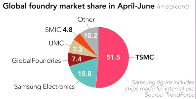
market share of players

fascinating book

“If (when!) it works it’s going to be glorious, but that’s not to underestimate the challenges of getting there!”
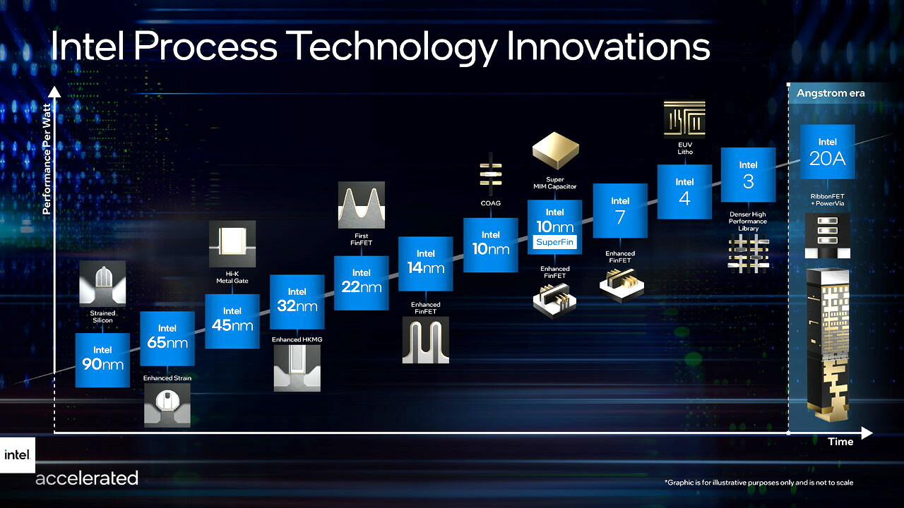
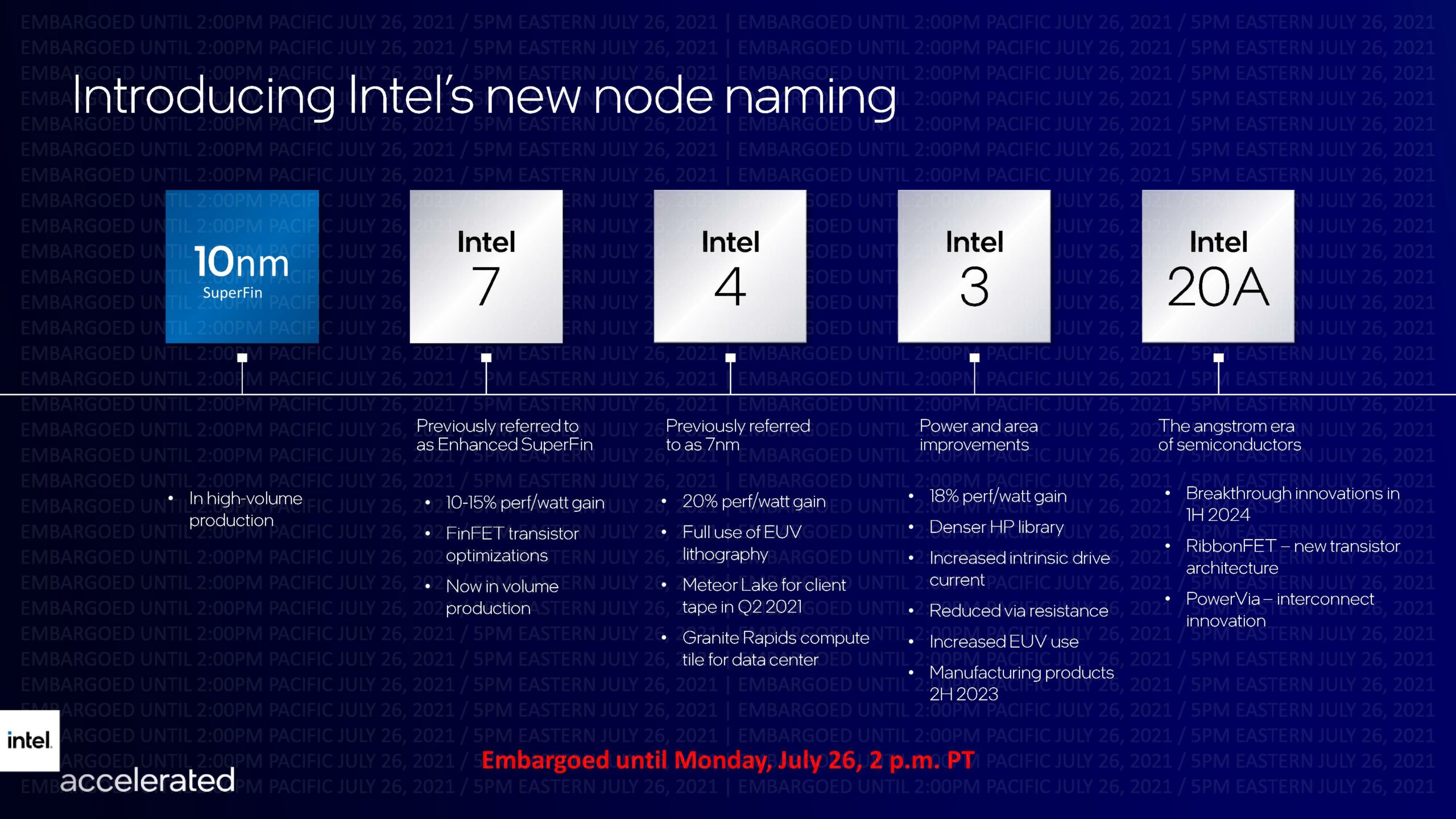
Ångstrom Era
when semiconducters are smaller than 1nm (nanometer)
1 Å = 0.1 nanometre = 100 picometres
“Although deprecated by both the International Bureau of Weights and Measures (BIPM) and the US National Institute of Standards and Technology (NIST), the unit is still often used in the natural sciences and technology to express sizes of atoms, molecules, microscopic biological structures, and lengths of chemical bonds, arrangement of atoms in crystals, wavelengths of electromagnetic radiation, and dimensions of integrated circuit parts” (src: Wiki)
why did intel not go with picometers then? 🤔 (ANGST!)
“Cautions In Using High-NA EUV”
Frederick Chen (Advanced Memory Development at Winbond Electronics)
Published Sep 20, 2021
“High-NA EUV has received a lot of attention ever since Intel put the spotlight on its receiving the first 0.55 NA EUV tool from ASML [1], expected in 2025. EUV itself has numerous issues which have been enumerated by myself and others, most notoriously the stochastic defects issue. There are also a host of issues related to the propagation of the EUV light in 3D through the mask topology, with shadowing being the easiest description of the phenomenon [2]. It has already been disclosed by one EDA vendor, in fact, that EUV is being practiced with multipatterning [3], defeating the purpose for which it was originally intended. So, with the entry of high-NA EUV, the prospect of single patterning EUV makes it a very attractive option. What changes can we aspect with a high-NA EUV system compared to the current EUV system?”
“Improvements with High NA”
“The high NA increases the numerical aperture (NA) from the current value of 0.33 to 0.55. The first benefit is this decreases the minimum optical spot size to 60% of its current value. The nominal value is given by the Rayleigh criterion of 0.61*nominal wavelength(=13.5 nm)/NA, which is 25 nm for 0.33 NA and 15 nm for 0.55 NA. This, of course, helps gives a sharper aerial image, i.e., the classically projected image at the focused point in space. In reality, the image is noisier due to the limited number of photons and blurred by electrons and chemical species in the resist.
A second benefit from the high-NA system is the increased demagnification in the Y-direction (from 4X to 8X). This has the effect of reducing the spread of angles. Keeping the original 4X would have resulted in a prohibitive range of angles. This helps reduce the impact of the 3D propagation through the mask mentioned earlier. Furthermore, since the X-demagnification is the same, there is also a reduction in the range of azimuthal rotation of the plane of incidence through the slit. The illumination sine ratio (kx/4)/(ky/8) = 2 kx/ky on the mask is halved to kx/ky on the wafer, whereas for the current imaging systems the same ratio (kx/4)/(ky/4) on the mask is preserved as kx/ky on the wafer. Thus, this improves the illumination consistency through the slit.
Complications/Tradeoffs with High NA
There are three issues with the move to a higher NA. The first should be well-known to lithographers, since it is the reduced depth of focus [4]. While the 0.33 NA 13.5 nm wavelength gives a depth of focus of 120 nm, increasing the NA to 0.55 reduces the depth of focus to a third of that, 41 nm.
The second issue is a consequence of the 8x Y-demagnification. Since the EUV mask 104 mm x 132 mm field size is not changing, the scanned field on the wafer has to be halved (in Y) from 26 mm x 33 mm to 26 mm x 16.5 mm. If a chip pattern originally took up over half the 26 mm x 33 mm field (as usually the case, even as 3 x 3 dies, for example), it would be chopped midway, leading to the need to stitch the two parts together through the exposure of two masks. Hence, double exposure patterning may creep in, spoiling the single patterning scenario.
The third issue is definitely a gotcha, since it was supposed to have been avoided at all costs in previous lithography system designs. The use of larger mirrors in the high-NA EUV system has led to unavoidable obscuration, where one mirror cannot avoiding blocking another. This has fundamental optical consequences, particularly reduction of modulation at lower spatial frequencies [5]. In some cases, the effects can be very drastic. In the example of a staggered 40 nm x 70 nm array below, one of the diffraction orders is obstructed by the central obscuration in the pupil of the 0.55 NA system.”

“In this example, it would lead to a doubling of the spatial frequency in the y-direction, which is a basic imaging error. The required modulation of the fundamental spatial frequency in the y-direction is eliminated when it should be kept for this pattern. Since much of the pupil is covered by forbidden illumination zones (shown in pink), this is difficult to integrate with other patterns which normally require more flexible illumination. For larger pitches of the same staggered array pattern, the zones would crowd closer together, allowing even less flexibility. This is something the high-NA EUV user has to be especially aware of.
No, stochastics will not go away
The use of higher NA reduces the spot size, and hence, the image pixel size is also effectively reduced. We also expect the resist blur to be reduced in order to take advantage of higher resolution. Hence, at the same dose and k1 (feature size normalized to wavelength/NA), the number of photons in the same number of edge pixels will continue to decrease. This means the stochastic issues of EUV imaging will persist at the feature edge.”
“References
[2] A. Erdmann et al., “3D mask effects in high NA EUV imaging,” Proc. SPIE 10957, 109570Z (2019).
[3] https://www.ednasia.com/multi-patterning-strategies-for-navigating-the-sub-5-nm-frontier-part-3/
[4] B. J. Lin, “The k3 coefficient in nonparaxial l/NA scaling equations for resolution, depth of focus, and immersion lithography” J. Micro/Nanolith. MEMS MOEMS 1(1) 7–12 (April 2002).
[5] S. T. Yang et al., “Effect of central obscuration on image formation in projection lithography,” Proc. SPIE 1264, 477 (1990).”
src: linkedin.com
Links:
https://www.imec-int.com/en/articles/high-na-euvl-next-major-step-lithography
#linux #gnu #gnulinux #opensource #administration #sysops #cpu #hardware #amd #intel #ai #superpower #china #taiwan #asml #tsmc #arm
Originally posted at: https://dwaves.de/2021/11/13/ai-superpowers-china-silicon-valley-and-the-new-world-order-kai-fu-lee-light-and-silicon-extreme-ultra-violet-cpu-production-asml-netherlands-tsmc-taiwan-amd-intel-usa-and-the-crazy-phys/
One person like that
fascinating video(s)
thanks for making & sharing 🙂 will do the best to assemble an informative article 🙂
https://ytpak.net/watch?v=CkNn98WE5_k
https://ytpak.net/watch?v=oIiqVrKDtLc
market share of players
fascinating book
https://duckduckgo.com/?q=China+Silicon+Valley+And+The+New+World+&ia=web
“If (when!) it works it’s going to be glorious, but that’s not to underestimate the challenges of getting there!”
Ångstrom Era
when semiconducters are smaller than 1nm (nanometer)
1 Å = 0.1 nanometre = 100 picometres
“Although deprecated by both the International Bureau of Weights and Measures (BIPM) and the US National Institute of Standards and Technology (NIST), the unit is still often used in the natural sciences and technology to express sizes of atoms, molecules, microscopic biological structures, and lengths of chemical bonds, arrangement of atoms in crystals, wavelengths of electromagnetic radiation, and dimensions of integrated circuit parts” (src: Wiki)
why did intel not go with picometers then? 🤔 (ANGST!)
“Cautions In Using High-NA EUV”
Frederick Chen (Advanced Memory Development at Winbond Electronics)Published Sep 20, 2021
“High-NA EUV has received a lot of attention ever since Intel put the spotlight on its receiving the first 0.55 NA EUV tool from ASML [1], expected in 2025. EUV itself has numerous issues which have been enumerated by myself and others, most notoriously the stochastic defects issue. There are also a host of issues related to the propagation of the EUV light in 3D through the mask topology, with shadowing being the easiest description of the phenomenon [2]. It has already been disclosed by one EDA vendor, in fact, that EUV is being practiced with multipatterning [3], defeating the purpose for which it was originally intended. So, with the entry of high-NA EUV, the prospect of single patterning EUV makes it a very attractive option. What changes can we aspect with a high-NA EUV system compared to the current EUV system?”
“Improvements with High NA”
“The high NA increases the numerical aperture (NA) from the current value of 0.33 to 0.55. The first benefit is this decreases the minimum optical spot size to 60% of its current value. The nominal value is given by the Rayleigh criterion of 0.61*nominal wavelength(=13.5 nm)/NA, which is 25 nm for 0.33 NA and 15 nm for 0.55 NA. This, of course, helps gives a sharper aerial image, i.e., the classically projected image at the focused point in space. In reality, the image is noisier due to the limited number of photons and blurred by electrons and chemical species in the resist.
A second benefit from the high-NA system is the increased demagnification in the Y-direction (from 4X to 8X). This has the effect of reducing the spread of angles. Keeping the original 4X would have resulted in a prohibitive range of angles. This helps reduce the impact of the 3D propagation through the mask mentioned earlier. Furthermore, since the X-demagnification is the same, there is also a reduction in the range of azimuthal rotation of the plane of incidence through the slit. The illumination sine ratio (kx/4)/(ky/8) = 2 kx/ky on the mask is halved to kx/ky on the wafer, whereas for the current imaging systems the same ratio (kx/4)/(ky/4) on the mask is preserved as kx/ky on the wafer. Thus, this improves the illumination consistency through the slit.
Complications/Tradeoffs with High NA
There are three issues with the move to a higher NA. The first should be well-known to lithographers, since it is the reduced depth of focus [4]. While the 0.33 NA 13.5 nm wavelength gives a depth of focus of 120 nm, increasing the NA to 0.55 reduces the depth of focus to a third of that, 41 nm.
The second issue is a consequence of the 8x Y-demagnification. Since the EUV mask 104 mm x 132 mm field size is not changing, the scanned field on the wafer has to be halved (in Y) from 26 mm x 33 mm to 26 mm x 16.5 mm. If a chip pattern originally took up over half the 26 mm x 33 mm field (as usually the case, even as 3 x 3 dies, for example), it would be chopped midway, leading to the need to stitch the two parts together through the exposure of two masks. Hence, double exposure patterning may creep in, spoiling the single patterning scenario.
The third issue is definitely a gotcha, since it was supposed to have been avoided at all costs in previous lithography system designs. The use of larger mirrors in the high-NA EUV system has led to unavoidable obscuration, where one mirror cannot avoiding blocking another. This has fundamental optical consequences, particularly reduction of modulation at lower spatial frequencies [5]. In some cases, the effects can be very drastic. In the example of a staggered 40 nm x 70 nm array below, one of the diffraction orders is obstructed by the central obscuration in the pupil of the 0.55 NA system.”
“In this example, it would lead to a doubling of the spatial frequency in the y-direction, which is a basic imaging error. The required modulation of the fundamental spatial frequency in the y-direction is eliminated when it should be kept for this pattern. Since much of the pupil is covered by forbidden illumination zones (shown in pink), this is difficult to integrate with other patterns which normally require more flexible illumination. For larger pitches of the same staggered array pattern, the zones would crowd closer together, allowing even less flexibility. This is something the high-NA EUV user has to be especially aware of.
No, stochastics will not go away
The use of higher NA reduces the spot size, and hence, the image pixel size is also effectively reduced. We also expect the resist blur to be reduced in order to take advantage of higher resolution. Hence, at the same dose and k1 (feature size normalized to wavelength/NA), the number of photons in the same number of edge pixels will continue to decrease. This means the stochastic issues of EUV imaging will persist at the feature edge.”
“References
[2] A. Erdmann et al., “3D mask effects in high NA EUV imaging,” Proc. SPIE 10957, 109570Z (2019).
[3] https://www.ednasia.com/multi-patterning-strategies-for-navigating-the-sub-5-nm-frontier-part-3/
[4] B. J. Lin, “The k3 coefficient in nonparaxial l/NA scaling equations for resolution, depth of focus, and immersion lithography” J. Micro/Nanolith. MEMS MOEMS 1(1) 7–12 (April 2002).
[5] S. T. Yang et al., “Effect of central obscuration on image formation in projection lithography,” Proc. SPIE 1264, 477 (1990).”
src: linkedin.com
Links:
https://www.imec-int.com/en/articles/high-na-euvl-next-major-step-lithography
#linux #gnu #gnulinux #opensource #administration #sysops #cpu #hardware #amd #intel #ai #superpower #china #taiwan #asml #tsmc #arm
Originally posted at: https://dwaves.de/2021/11/13/ai-superpowers-china-silicon-valley-and-the-new-world-order-kai-fu-lee-light-and-silicon-extreme-ultra-violet-cpu-production-asml-netherlands-tsmc-taiwan-amd-intel-usa-and-the-crazy-phys/