#semiconductors

waynerad@diasp.org

"Micron breaks out a fast 60TB SSD for mega data centers"

60TB, holy moly that's huge. Speed is 12 GB/s while using just 20 watts of power. Well, 12 GB/s is the read speed. 5 GB/s for writing. That's still fast enough that the whole drive can be fully written in just 3.4 hours.

"The 6550 ION also excels in critical AI training workloads compared to competitive 60TB SSDs, achieving:"

"147% higher performance for NVIDIA Magnum IO GPUDirect Storage (GDS) and 104% better energy efficiency",

"30% higher 4KB transfer performance for deep learning IO Unet3D testing and 20% better energy efficiency,

"151% improvement in completion times for AI model checkpointing while competitors consume 209% more energy."

Nvidia Magnum IO GPUDirect Storage is a technique invented by Nvidia that enables data to flow from memory (NVMe) to the GPU without having to pass through the CPU.

Apparently they used Unet3D to test it. Unet3D is a video segmentation model. Video segmentation means for each frame of the video, it "segments" pixels into groups that all belong to the same concept, for example one segment might be "road", another might be "sidewalk", and another might be "yard", etc. It's based an a "U-net" architecture, so called because it has a large input layer that gets progressively smaller until some encoding is output, which then goes into a series of layers that get progressively bigger until the output which is the same size as the input. You can think of the input as going "down" one side of a "U" to the endcoding, then "up" the other side of the "U" to the output, hence the name "U-net".

Micron breaks out a fast 60TB SSD for mega data centers

#solidstatelife #semiconductors #ssds #ai

waynerad@diasp.org

"Taiwan's technology protection rules prohibits Taiwan Semiconductor Manufacturing Co (TSMC) from producing 2-nanometer chips abroad, so the company must keep its most cutting-edge technology at home, Minister of Economic Affairs J.W. Kuo."

"Kuo made the remarks in response to concerns that TSMC might be forced to produce advanced 2-nanometer chips at its fabs in Arizona ahead of schedule after former US president Donald Trump was re-elected as the next US president."

TSMC cannot make 2nm chips abroad now: MOEA

#solidstatelife #semiconductors #geopolitics

waynerad@diasp.org

"No more nanometers: It's time for new node naming", says Kevin Morris.

"Intel held the line from '10 micron' in 1972 through '0.35 micron' in 1995, an impressive 23-year run where the node name matched gate length. Then, in 1997 with the '0.25 micron/250 nm' node they started over-achieving with an actual gate length of 200 nm -- 20% better than the name would imply. This 'sandbagging' continued through the next 12 years, with one node (130nm) having gate length of only 70nm -- almost a 2x buffer. Then, in 2011, Intel jumped over to the other side of the ledger, ushering in what we might call the 'overstating decade' with the '22nm' node sporting a gate length of 26 nm. Since then, things have continued to slide further in that direction, with the current '10nm' node measuring in with a gate length of 18 nm -- almost 2x on the other side of the 'named' dimension."

"So essentially, since 1997, the node name has not been a representation of any actual dimension on the chip, and it has erred in both directions by almost a factor of 2."

"For the last few years, this has been a big marketing problem for Intel from a 'perception' point of view. Most industry folks understand that Intel's '10nm' process is roughly equivalent to TSMC and Samsung's '7nm' processes. But non-industry publications regularly write that Intel has 'fallen behind' because they are still back on 10nm when other fabs have 'moved on to 7nm and are working on 5nm.' The truth is, these are marketing names only, and in no way do they represent anything we might expect in comparing competing technologies."

He mentions a proposal from Philip Wong of TSMC. His proposal is you replace "nanometers" with 3 numbers that reflect the actual usefulness of the chip: density of logic transistors in number per square millimeter, density of off-chip DRAM memory in bits per square millimeter, and density of connections between the memory and the logic transistors, in number of interconnects per square millimeter. So a chip could be described as: "DL: 38M, DM: 383M, DC: 12K", or just "38M, 383M, 12K".

That proposal was made in 2020 and so far, hasn't caught on. Maybe it's tough to market as it's not as exciting as a single single-digit number like "5 nm"? But "nanometers" needs to be replaced by something.

I looked online for a website with nice tables of those three numbers for all the recent chips. Couldn't find it.

It looks like these metrics are often kept secret by semiconductor companies to try to get a competitive advantage, but people say there are websites that have information on new chips and the underlying technology, such as WikiChip, SemiWiki, AnandTech, Tom's Hardware, IEDM, VLSI Symposium, IEEE Xplore, EE Times, Nature Electronics, IEEE International Roadmap for Devices and Systems, Semiconductor Industry Association, and so on. (Links to some of these below. I haven't had time to delve too deeply into any of these sites.)

No more nanometers: It's time for new node naming

#solidstatelife #semiconductors

waynerad@diasp.org

Export controls not working on semiconductor equipment to China.

"Huawei has been able to scoot around TSMC's weak end customer checks and secure thousands of leading edge wafers through Bitmain / Sophgo, and many other established Chinese design firms. While this is a huge failure in enforcement of the export controls, it's also relatively low volume compared to domestic fabrication of the Ascend 910B. Huawei has been relying on primarily Semiconductor Manufacturing International Corporation (SMIC) to produce their domestic AI chip and they have run tens of thousands of wafers of the main compute chiplet on their domestic SMIC N+2 (~7nm) and N+3 (~6nm) process nodes."

"SMIC produces 7nm-class chips including the Kirin 9000S mobile system-on-chip (SoC) and Ascend 910B AI accelerator. Two of their fabs are connected via wafer bridge, such that an automated overhead track can move wafers between them. For production purposes, this forms a continuous cleanroom and effectively one fab. But for regulatory purposes, they are separate! One building is entity-listed by the US and working on advanced logic for AI chips, a clear national security concern. The other is free to import 'dual use' tools as it runs only 'legacy processes.' Do you believe they aren't sharing anything over the wafer bridge?"

"An isotropic etch chamber, essential to producing the latest 2nm Gate-All-Around transistors, cannot be exported to China from Lam's US factories. This same etch chamber, manufactured in Lam's Malaysia facility, can legally be sold to an advanced logic fab in China if no US persons are involved (in manufacturing, sales, installation, and servicing). This includes even customers on the US entity list. Other companies follow the same playbook, including Applied Materials & KLA with their Singapore facilities."

"ChangXin Memory Technologies (CXMT)'s advanced DRAM with 18nm half pitch was subject to the original 2022 export controls. A new method of calculating half-pitch in the 2023 rules put them back above the minimum line for controls. Without changing the underlying process, they went from restricted to not. They also changed the node name from 17nm or 18.5nm to 19nm, to avoid any appearance of impropriety. The subtleties of the rule change that so specifically moved them from under to a literal nanometer or two over the restriction are, at least, very fortunate for CXMT. Lobbying efforts by giants such as Applied Materials who has made over $3 billion from CXMT may be noteworthy."

"Pengjin High-Tech, a gallium nitride (GaN) startup that is not entity-listed, is building its cleanroom across the street from entity-listed advanced logic producer Peng Xin Wei (PXW). Pengjin is free to import nearly all advanced Western production equipment, including equipment critical to producing advanced logic at 7nm or below (again the exceptions are a small number of tools on the control list, including extreme ultraviolet (EUV))."

Fab whack-a-mole: Chinese companies are evading US sanctions

#solidstatelife #semiconductors #geopolitics

waynerad@diasp.org

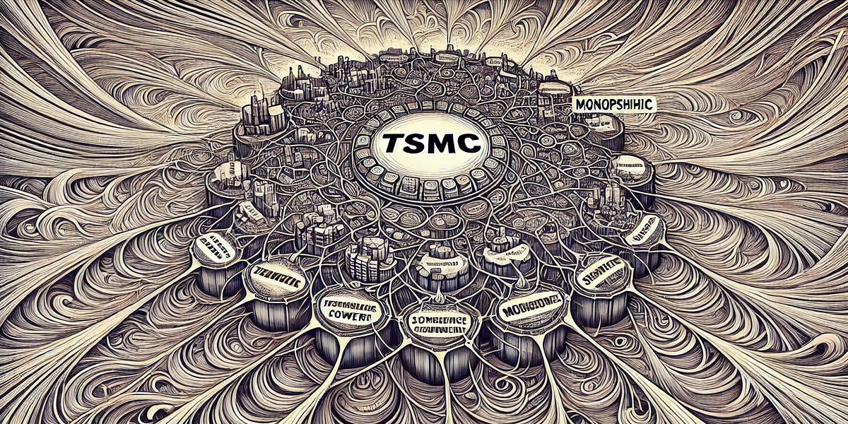
"TSMC isn't a pure monopsony in the wafer fab equipment market. Intel and Samsung are still buying tools, just not as often as wafer fab equipment manufacturers would like. Memory manufacturers also buy wafer fab equipment tools, and trailing-edge foundries do too."

"Monopsony refers to a market in which there is only a single buyer, i.e., producers cannot find alternative buyers of their product."

"Monopsony permits the buyer to establish prices, terms and conditions that are quite different from those that would result from a market structure in which there were many competing buyers and sellers."

The only seller the article mentions is ASML. Single-seller market, too? At least when it comes to high-numeric-aperture (high-NA) extreme ultraviolet (EUV) lithography tools.

"When there are only a few buyers, it's an oligopsony. Given the consolidated nature of the semiconductor industry, most markets within the semiconductor supply chain are already oligopsonistic."

Monopsony and TSMC

#solidstatelife #semiconductors

waynerad@diasp.org

"How AlphaChip transformed computer chip design."

"AlphaChip" is the name Google has bestowed on their reinforcement learning system for doing chip layouts for semiconductor manufacturing.

It's dramatically accelerating the pace of chip design by dramatically shortening the time it takes to door the chip "floorplanning" process, with results superior to what human designers can do.

"Similar to AlphaGo and AlphaZero, which learned to master the games of Go, chess and shogi, we built AlphaChip to approach chip floorplanning as a kind of game."

"Starting from a blank grid, AlphaChip places one circuit component at a time until it's done placing all the components. Then it's rewarded based on the quality of the final layout. A novel "edge-based" graph neural network allows AlphaChip to learn the relationships between interconnected chip components and to generalize across chips, letting AlphaChip improve with each layout it designs."

"AlphaChip has generated superhuman chip layouts used in every generation of Google's TPU since its publication in 2020. These chips make it possible to massively scale-up AI models based on Google's Transformer architecture."

"TPUs lie at the heart of our powerful generative AI systems, from large language models, like Gemini, to image and video generators, Imagen and Veo. These AI accelerators also lie at the heart of Google's AI services and are available to external users via Google Cloud."

"To design TPU layouts, AlphaChip first practices on a diverse range of chip blocks from previous generations, such as on-chip and inter-chip network blocks, memory controllers, and data transport buffers. This process is called pre-training. Then we run AlphaChip on current TPU blocks to generate high-quality layouts. Unlike prior approaches, AlphaChip becomes better and faster as it solves more instances of the chip placement task, similar to how human experts do."

"With each new generation of TPU, including our latest Trillium (6th generation), AlphaChip has designed better chip layouts and provided more of the overall floorplan, accelerating the design cycle and yielding higher-performance chips."

"Beyond designing specialized AI accelerators like TPUs, AlphaChip has generated layouts for other chips across Alphabet, such as Google Axion Processors, our first Arm-based general-purpose data center CPUs."

"External organizations are also adopting and building on AlphaChip. For example, MediaTek, one of the top chip design companies in the world, extended AlphaChip to accelerate development of their most advanced chips -- like the Dimensity Flagship 5G used in Samsung mobile phones -- while improving power, performance and chip area."

How AlphaChip transformed computer chip design - Google DeepMind

#solidstatelife #ai #reinforcementlearning #semiconductors

waynerad@diasp.org

I just discovered there's a "Hacker Fab" at Carnegie Mellon University (CMU) that is producing a completely open-source system for photolithography -- so all the equipment you need to build your own photolithography tools and manufacture your own chips, you can build yourself from open-source designs.

I learned this from a video, by a guy who decided to build his own photolithography system in his garage, so I decided I'll just give you the video. (I'll put a link to the Hacker Fab below.) The main impression I got from the video is, if you wanted to build your own photolithography system, you'd spend countless hours getting tiny details right -- getting the focus exactly right, getting the alignment of things exactly right, etc. (He promises an additional video with even more of these details -- he says he cut a lot to make this one, and it's still 45 min long.) People in the semiconductor industry have literally spent decades getting all these details right so you can have your chips.

In the end, he manages to create a photolithography setup capable of manufacturing circa-1980-era chips, with a 1 micron minimum feature size -- er, almost. He didn't quite make 1 micron. A long way from the state of the art but still pretty impressive, and 1980-era chips are still used in embedded systems and such -- they're not entirely useless and haven't entirely gone away.

Speedrunning 30yrs of lithography technology - Breaking Taps

#solidstatelife #semiconductors

waynerad@diasp.org

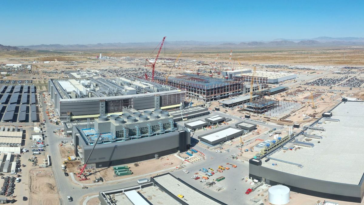
"Eyepopping factory construction boom in the US"

"Companies plowed $18.4 billion in April into the construction of manufacturing plants in the US, a seasonally adjusted annual rate of construction spending of a record $212 billion, according to the Census Bureau today. This was up by 140% to 200% from the range in 2015 through mid-2021."

"TSMC has announced over $65 billion in investments, including $40 billion for two fabs that are now under construction near Phoenix."

"Intel has rolled out $100 billion in investment plans, including $43 billion for facilities in Ohio, New Mexico, Oregon, and Arizona."

"Texas Instruments is investing $30 billion in Texas."

"Samsung..." "Micron..." "Toyota..." "Kohler..." "Crystal Window & Door Systems..." "ION Storage Systems..." "GAF Energy..." "GF Casting Solutions..." "Boviet Solar..." "Green New Energy Materials..."

Eyepopping factory construction boom in the US

#economics #construction #semiconductors

carstenraddatz_fca@nerdica.net

What I look for in interviews

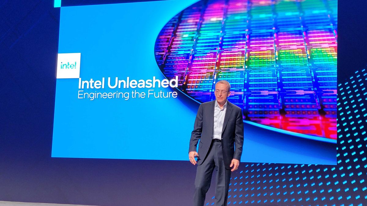
So consultant Ian Cutress, who has a side business on youtube, gets to interview Pat Gelsinger, of 486 fame and effing Intel CEO. After he gave a keynote (Gelsinger, not Cutress, that is).

The strategic views are good and rich, but as those centre closely around the technologies in use today, the ex chip designer feels authentic to me. Specifically in moments around, say, 7:32 when its about Foveros Direct, and 9:01 when advanced packaging is on topic, "nice and simple". Or just when he says, understatement galore, that he is "judge and jury" on this decision of this or that, and how to lower customer's risks at 12:14.

While listening, keeping his features in check, he looks as stressed as any other CEO. Fully professional. But I sense the authenticity of an engineer, which I dig. Just sayin'.

https://www.youtube.com/watch?v=0PrmrMQ9gJU

#semiconductors #ceospeak #intel #semicon #interview

waynerad@diasp.org

"Intel unveiled a new roadmap that includes a new 14A node, the industry's first to use High-NA EUV, here at its Intel Foundry Services Direct Connect 2024 event."

Intel no longer uses "nanometers" to refer to its "process nodes", so I don't know what "14A" means, but, there is a quote somewhere of Intel CEO Pat Gelsinger saying 14A produces "1.4 nanometer technology." Maybe "14A" means 14 angstroms.

The other term in there is "High-NA EUV". "NA" stands for "numerical aperture". But to understand the significance of that we have to take a few steps back.

The company that makes the semiconductor manufacturing equipment is ASML (Advanced Semiconductor Materials Lithography).

Chips are made through a process called photolithography, which involves shining light through a chip design in such a way that it is miniaturized, and through a process using a lot of complicated chemistry, that pattern can be etched into the surface of the silicon and turned into an electronic circuit. These circuits have gotten so small that visible light has wavelengths too big to make the chip. Chipmakers predictably went to ultraviolet light, which has shorter wavelengths. That worked for a time, but suddenly a problem came up, which is that air was opaque to the wavelengths they wanted to use.

To us, we think of air as transparent, and for the visible wavelengths that our eyes use, it is pretty much perfectly transparent. But it is not transparent at all wavelengths. At certain ultraviolet wavelengths, it's opaque like black smoke.

This is why the semiconductor industry had to make the sudden jump from using lasers that emit light at 193 nanometers to lasers that emit light at 13.5 nanometers. (13.5 was chosen because people just happened to know how to make light at that frequency with a tin plasma laser.) Jumping the chasm from 193 to 13.5 jumps across the wavelengths where air is opaque. 193 has been called "deep ultraviolet", or DUV. 13.5 is called "extreme ultraviolet", or EUV. So whenever you see "EUV", which we see here in the phrase "Nigh-NA EUV", that's what it's talking about.

Making this jump required rethinking all the optics involved in making chips. Mainly this involved replacing all the lenses with mirrors. Turns out at 13.5 nanometers, it's easier to do optics with reflective mirrors than transparent lenses.

Besides decreasing the wavelength (and increasing the frequency) of the light, what else can be done?

It turns out there's two primary things that determine the limit of the size you cat etch: the light wavelength and the numerical aperture. There's some additional factors that have to do with the chemistry you're using for the photoresists and so fourth, but we'll not concern ourselves with those factors at the moment.

So what is numerical aperture? If you're a photographer, you probably already know, but it has to do with the angle at which a lens can collect light.

"The numerical aperture of an optical system such as an objective lens is defined by:

NA = n sin(theta)

where n is the index of refraction of the medium in which the lens is working (1.00 for air, 1.33 for pure water, and typically 1.52 for immersion oil), and theta is the half-angle of the maximum cone of light that can enter or exit the lens."

As for "the medium in which the lens is working", note that ASML used water immersion with deep ultraviolet (193 nanometer light and higher) to achieve an NA greater than 1. This hasn't been done for extreme ultraviolet (13.5 nanometer light).

The increase in numerical aperture that ASML has recently accomplished, and that Intel is announcing they are using, is an increase from 0.33 to 0.55. (Numerical aperture is a dimensionless number.)

How did ASML achieve this increase? Their page on "5 things you should know about High NA EUV lithography" (link below) gives a clue. One of the 5 things is, "larger, anamorphic optics for sharper imaging".

The page refers to "EXE" and "NXE". These refer to ASML's own equipment. NXE systems have a numerical aperture of 0.33, but with the EXE systems, ASML has increased it to 0.55.

"Implementing this increase in NA meant using bigger mirrors. But the bigger mirrors increase the angle at which light hit the reticle, which has the pattern to be printed."

You're probably not familiar with the term "reticle". Here the meaning is different from normal optics. In normal optics, it refers to a scale that you might see in a microscope scope. But here, it has to do with the fact that chips are no longer manufactured with the entire pattern for the whole chip all in one shot. Instead, a pattern for only a small portion of the wafer is used at a time, and then stepper motors move the wafer and the process is repeated. This small portion of the pattern that is used at a time is called the "reticle".

"At the larger angle the reticle loses its reflectivity, so the pattern can't be transferred to the wafer. This issue could have been addressed by shrinking the pattern by 8x rather than the 4x used in NXE systems, but that would have required chipmakers to switch to larger reticles."

"Instead, the EXE uses an ingenious design: anamorphic optics. Rather than uniformly shrinking the pattern being printed, the system's mirrors demagnify it by 4x in one direction and 8x in the other. That solution reduced the angle at which the light hit the reticle and avoided the reflection issue. Importantly, it also minimized the new technology's impact on the semiconductor ecosystem by allowing chipmakers to continue using traditionally sized reticles."

Intel announces new roadmap at IFS Direct Connect 2024: New 14A node, Clearwater Forest taped-in, five nodes in four years remains on track

#solidstatelife #mooreslaw #semiconductors

carstenraddatz_fca@nerdica.net

Seid umschlungen, Milliarden

Mal ein Interview mit einer interessanten Expertin zum Thema Industriepolitik und Subventionen in der FAZ. Mariana Mazzzcato kannte ich zuvor nicht, aber ich streife das Feld ja auch nur.

Meine Lesart trifft das: was sie sagt Recht gut.

Europa braucht mehr Unabhängigkeit bei Halbleitern, und das Dutzend Milliarden ist gut investiert, vor allem dann wenn es denn gut investiert ist und auch in die Breite geht. Lies: Ausbildung und akademische Strukturen müssen mitgenommen werden. Hilft ja nix wenn Intel und die anderen alle kommen, aber deutschlandweit keine Köpfe nachwachsen. Wird das Unterfangen kein Generationennprojekt ist IPCEI II nur eine Luftnummer.

Link: https://m.faz.net/aktuell/wirtschaft/mehr-wirtschaft/mariana-mazzucato-habecks-lieblingsoekonomin-ueber-ihr-verhaeltnis-zum-minister-19509042.html (verschwindet bestimmt bald hinter Paywall)

Progressiv verstanden sollen Subventionen, so sie eigentlich als eine Anschubfinanzierung funktionieren, einen Rückfluss von Geld ermöglichen. Klingt besser als ein Tropf, aus dem ja eher keine Innovation zu erwarten ist. Ökosystem statt Gießkanne und Stickerwasser.

Mazzucato: Ich würde auch fordern: Wenn die Firma einen Gewinn macht, geht ein Teil davon zurück in den Innovationsfonds der Regierung. Auf solche Details kommt es an, wenn Sie ein schlauer unternehmerischer Staat sein wollen.FAZ: Was halten Sie von zehn Milliarden Euro für eine neue Intel-Fabrik in Magdeburg?

Das kann ich akzeptieren. Chip-Souveränität ist wichtig für Amerika und Europa, sonst kommen alle Chips aus Taiwan. Dies ist eine Chance, sicherzustellen, dass die Chipindustrie zu nachhaltigem Wachstum für alle beiträgt. Die USA machen ihr öffentliches Geld davon abhängig, dass die Unternehmen Arbeitsbedingungen verbessern, grüne Lieferketten verwenden und nicht nur Aktien zurückkaufen. Aber wie stellen Sie sicher, dass Sie über alle Aspekte nachdenken, über das ganze System? Dass man mit einer Subvention nicht ein neues Problem anderswo schafft?

Die Nachbarfirmen der neuen Intel-Fabrik in Magdeburg haben Angst, dass sie bald keine Mitarbeiter mehr finden.

Sie müssen systemisch denken, ein Ökosystem schaffen und nicht nur eine Firma subventionieren. Mit anderen Worten: Sie brauchen eine schlaue Industriepolitik, getrieben von einer Mission, die es zum Beispiel auch Start-ups ermöglicht, zu wachsen, statt nur einem großen Unternehmen eine Subvention zu zahlen.

#semiconductors #Europe #policy #Intel #Magdeburg #IPCEI #ipcei-ii

waynerad@diasp.org

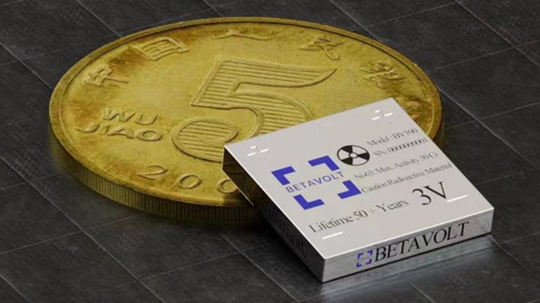
"Chinese-developed nuclear battery has a 50-year lifespan -- Betavolt BV100 built with Nickel-63 isotope and diamond semiconductor material."

"This 15 x 15 x 5mm battery delivers 100 microwatts at 3 volts. The company says multiple BV100 batteries can be used together in series or parallel depending on device requirements."

"The new BV100 is claimed to be a disruptive product on two counts. Firstly, a safe miniature atomic battery with 50 years of maintenance-free stamina is a breakthrough. Secondly, Betavolt claims it is the only company in the world with the technology to dope large-size diamond semiconductor materials, as used by the BV100."

Wow, I didn't even know diamond semiconductors were a thing.

"Betavolt says its atomic battery is very different from similarly described power cells developed by the US and USSR in the 1960s. It says that the old nuclear batteries were large, dangerous, hot, and expensive products. For example, some old-tech atomic batteries used Plutonium as the radioactive power source. Meanwhile, the Betavolt BV100 is claimed to be safe for consumers and won't leak radiation even if subjected to gunshots or puncture."

Chinese-developed nuclear battery has a 50-year lifespan -- Betavolt BV100 built with Nickel-63 isotope and diamond semiconductor material

#inventions #semiconductors #batteries

waynerad@diasp.org

Graphene as a semiconductor? I thought it was impossible to turn graphene into a semiconductor because it doesn't have a big enough band gap. But researchers have developed a technique for combining graphene with silicon carbide. The graphene has better heat dissipation at higher density than silicon.

I'll have a closer look at this at some unspecified time in the future, but for now I'll give you all this quick overview from Sabine Hossenfelder.

This new semiconductor could revolutionize computing - Sabine Hossenfelder

#solidstatelife #semiconductors #graphene

waynerad@diasp.org

"Teardown finds Huawei's 5nm notebook processor was made in Taiwan, not China."

"According to a teardown of Huawei's Qingyun L540 notebook by testers at TechInsights, the mysterious 5nm Kirin 9006C processor it contained was actually manufactured by Taiwan Semiconductor Manufacturing Co, not from a Middle Kingdom manufacturer."

"When the 14-inch ultralight first appeared in early December, the presence of a 5nm processor spurred furious speculation that China's domestic semiconductor manufacturing capability was far more advanced than previously thought."

Looks like the Chinese are not as advanced as I thought they might be.

Anyone here a Chinese chip expert, and want to explain the difference between Huawei's Kirin 9000S and 9006C?

Teardown finds Huawei's 5nm notebook processor was made in Taiwan, not China

#solidstatelife #semiconductors #huawei #china #tsmc