Choose your words wisely - or it may cost you...
Intel CEO Lost A 40% Discount For TSMC's Latest Chip Tech After Taiwan Remarks - Report https://wccftech.com/intel-ceo-lost-a-40-discount-for-tsmcs-latest-chip-tech-after-taiwan-remarks-report/
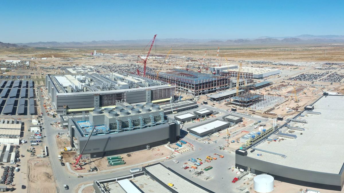
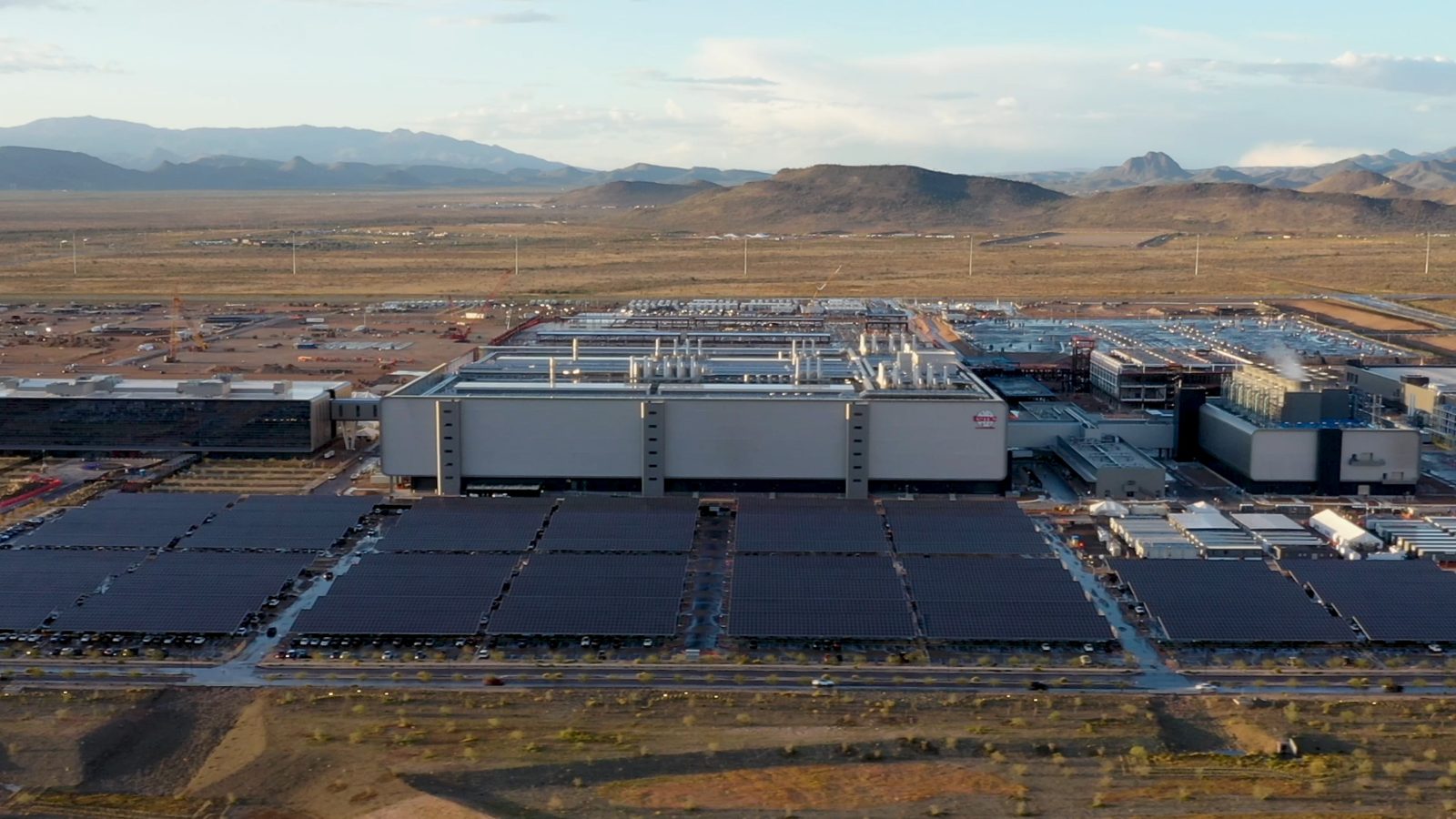
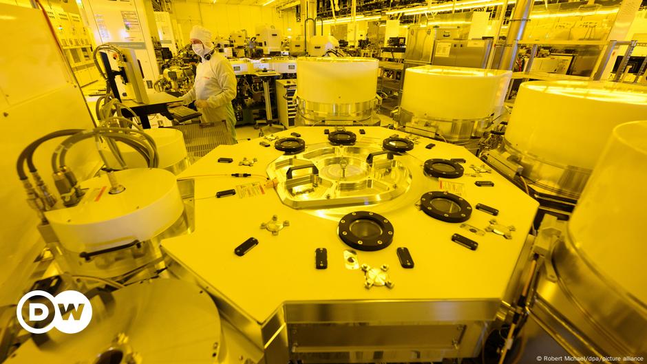
Intel CEO Patrick Gelsinger's comments about the Taiwan Semiconductor Manufacturing Company's (TSMC) manufacturing presence in China soured relations between the two firms and eventually led to Intel missing out on key discounts offered by TSMC, according to a fresh report from Reuters. Intel is currently focusing on manufacturing chips with its 18A manufacturing process, and Reuters' report shares that before Gelsinger's comments, TSMC was offering Intel a whopping 40% discount for its 3 nanometer process manufacturing family. However, the Taiwanese firm decided to withdraw the offer following Gelsinger's remarks.
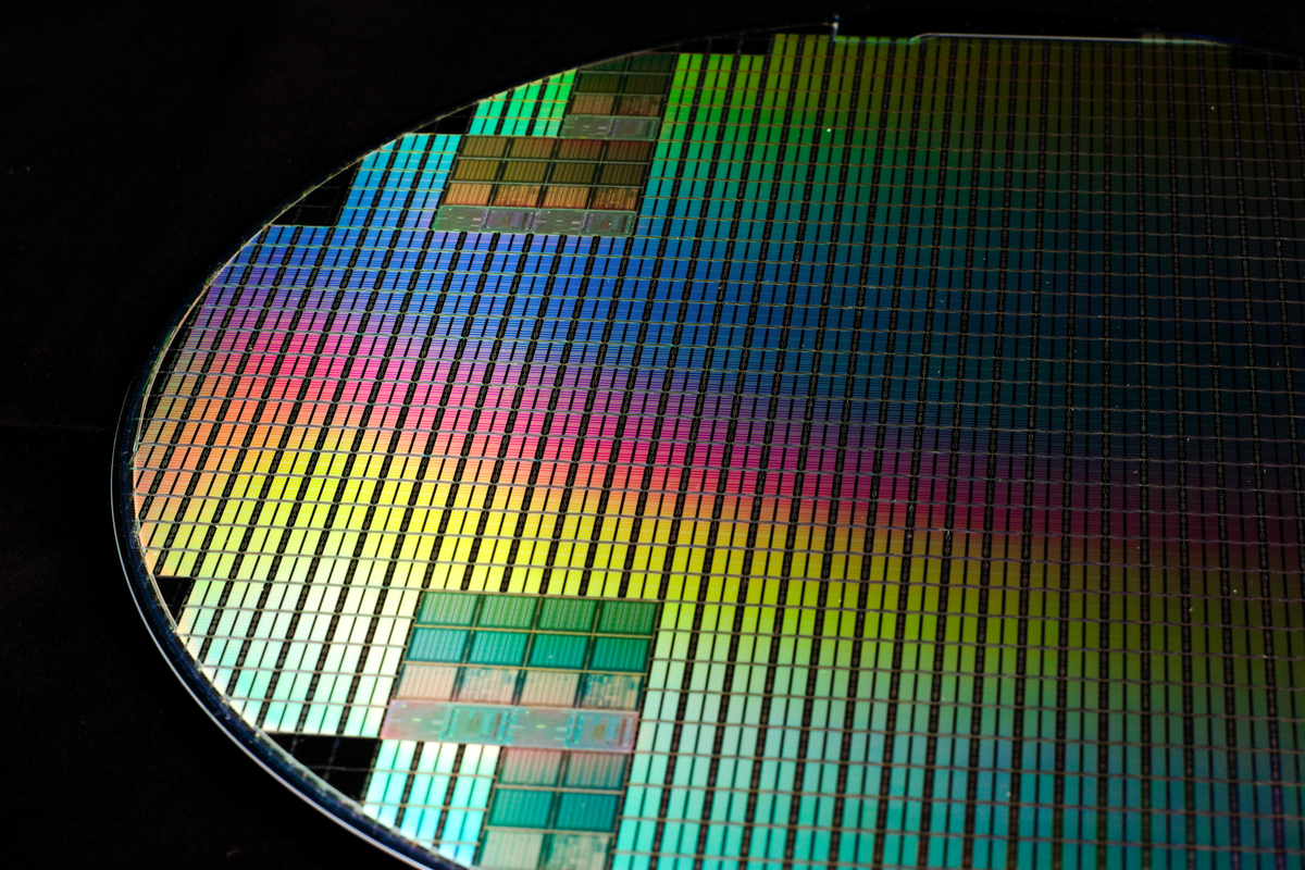
As per Reuters, in 2021, TSMC had offered Intel a stunning 40% discount for the 3 nanometer technology. Back then, 3 nanometers was TSMC's leading edge chip manufacturing process. One wafer cost $23,000 back then, and TSMC had offered Intel a 40% discount to bring the price to roughly $14,000.
However, back then, Intel was moving full speed ahead to attract US government subsidies for its contract manufacturing and advanced technology push. As part of the effort, Gelsinger was eagerly pointing out the geopolitical risks associated with advanced chip manufacturing being concentrated in Taiwan.
Some of his most controversial remarks, which ignited a back and forth with TSMC's outspoken founder, Dr. Morris Chang, were made at the Fortune Brainstorm Tech Conference in Half Moon Bay, California. At the event, Gelsinger commented that "Taiwan is not a stable place" adding that "Does that make you feel more comfortable or less?"