AI Superpowers China Silicon Valley and the New World Order - Kai-Fu Lee - light and silicon - extreme Ultra Violet CPU production - ASML (Netherlands) tsmc (Taiwan) AMD Intel (USA) and the crazy physics behind transition from 14nm to 7nm process - Ångstrom Era
fascinating video(s)
thanks for making & sharing 🙂 will do the best to assemble an informative article 🙂
https://ytpak.net/watch?v=CkNn98WE5_k
https://ytpak.net/watch?v=oIiqVrKDtLc
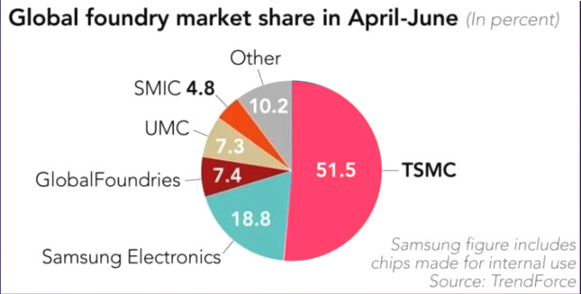
market share of players

fascinating book

https://duckduckgo.com/?q=China+Silicon+Valley+And+The+New+World+&ia=web
“If (when!) it works it’s going to be glorious, but that’s not to underestimate the challenges of getting there!”
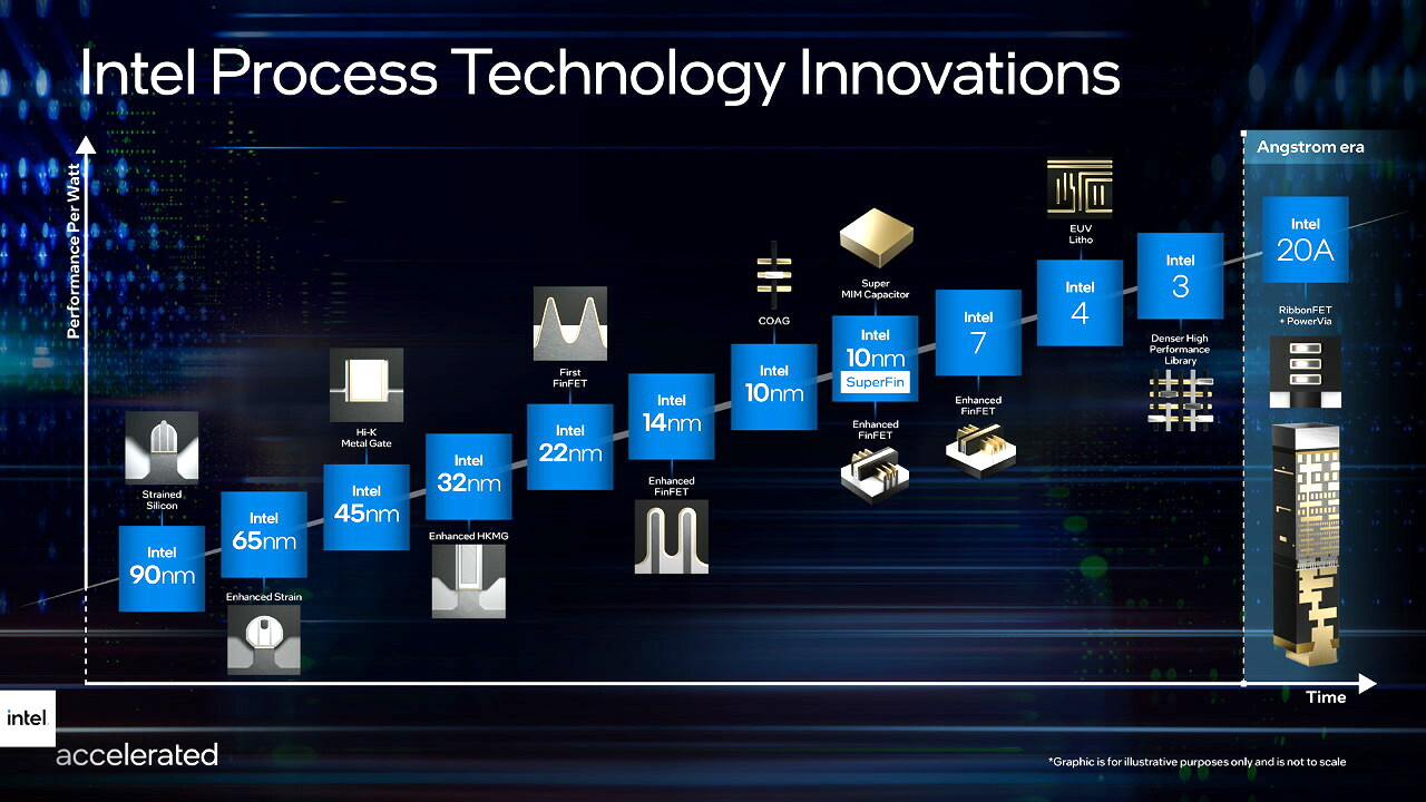
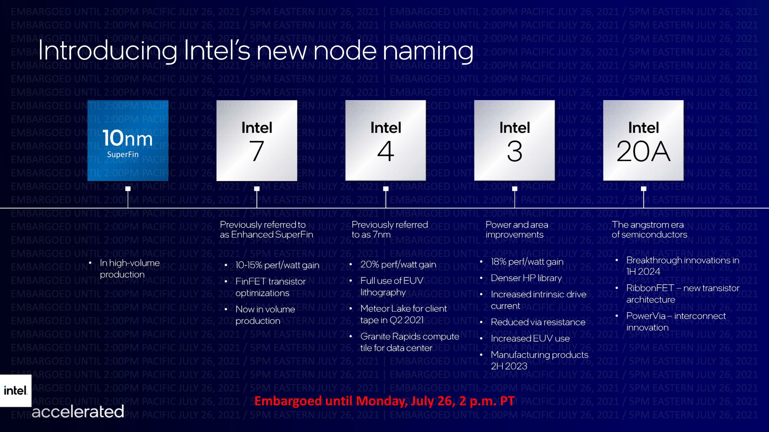
Ångstrom Era
when semiconducters are smaller than 1nm (nanometer)
1 Å = 0.1 nanometre = 100 picometres
“Although deprecated by both the International Bureau of Weights and Measures (BIPM) and the US National Institute of Standards and Technology (NIST), the unit is still often used in the natural sciences and technology to express sizes of atoms, molecules, microscopic biological structures, and lengths of chemical bonds, arrangement of atoms in crystals, wavelengths of electromagnetic radiation, and dimensions of integrated circuit parts” (src: Wiki)
why did intel not go with picometers then? 🤔 (ANGST!)
Frederick Chen (Advanced Memory Development at Winbond Electronics)Published Sep 20, 2021
“High-NA EUV has received a lot of attention ever since Intel put the spotlight on its receiving the first 0.55 NA EUV tool from ASML [1], expected in 2025. EUV itself has numerous issues which have been enumerated by myself and others, most notoriously the stochastic defects issue. There are also a host of issues related to the propagation of the EUV light in 3D through the mask topology, with shadowing being the easiest description of the phenomenon [2]. It has already been disclosed by one EDA vendor, in fact, that EUV is being practiced with multipatterning [3], defeating the purpose for which it was originally intended. So, with the entry of high-NA EUV, the prospect of single patterning EUV makes it a very attractive option. What changes can we aspect with a high-NA EUV system compared to the current EUV system?”
“Improvements with High NA”
“The high NA increases the numerical aperture (NA) from the current value of 0.33 to 0.55. The first benefit is this decreases the minimum optical spot size to 60% of its current value. The nominal value is given by the Rayleigh criterion of 0.61*nominal wavelength(=13.5 nm)/NA, which is 25 nm for 0.33 NA and 15 nm for 0.55 NA. This, of course, helps gives a sharper aerial image, i.e., the classically projected image at the focused point in space. In reality, the image is noisier due to the limited number of photons and blurred by electrons and chemical species in the resist.
A second benefit from the high-NA system is the increased demagnification in the Y-direction (from 4X to 8X). This has the effect of reducing the spread of angles. Keeping the original 4X would have resulted in a prohibitive range of angles. This helps reduce the impact of the 3D propagation through the mask mentioned earlier. Furthermore, since the X-demagnification is the same, there is also a reduction in the range of azimuthal rotation of the plane of incidence through the slit. The illumination sine ratio (kx/4)/(ky/8) = 2 kx/ky on the mask is halved to kx/ky on the wafer, whereas for the current imaging systems the same ratio (kx/4)/(ky/4) on the mask is preserved as kx/ky on the wafer. Thus, this improves the illumination consistency through the slit.
Complications/Tradeoffs with High NA
There are three issues with the move to a higher NA. The first should be well-known to lithographers, since it is the reduced depth of focus [4]. While the 0.33 NA 13.5 nm wavelength gives a depth of focus of 120 nm, increasing the NA to 0.55 reduces the depth of focus to a third of that, 41 nm.
The second issue is a consequence of the 8x Y-demagnification. Since the EUV mask 104 mm x 132 mm field size is not changing, the scanned field on the wafer has to be halved (in Y) from 26 mm x 33 mm to 26 mm x 16.5 mm. If a chip pattern originally took up over half the 26 mm x 33 mm field (as usually the case, even as 3 x 3 dies, for example), it would be chopped midway, leading to the need to stitch the two parts together through the exposure of two masks. Hence, double exposure patterning may creep in, spoiling the single patterning scenario.
The third issue is definitely a gotcha, since it was supposed to have been avoided at all costs in previous lithography system designs. The use of larger mirrors in the high-NA EUV system has led to unavoidable obscuration, where one mirror cannot avoiding blocking another. This has fundamental optical consequences, particularly reduction of modulation at lower spatial frequencies [5]. In some cases, the effects can be very drastic. In the example of a staggered 40 nm x 70 nm array below, one of the diffraction orders is obstructed by the central obscuration in the pupil of the 0.55 NA system.”

“In this example, it would lead to a doubling of the spatial frequency in the y-direction, which is a basic imaging error. The required modulation of the fundamental spatial frequency in the y-direction is eliminated when it should be kept for this pattern. Since much of the pupil is covered by forbidden illumination zones (shown in pink), this is difficult to integrate with other patterns which normally require more flexible illumination. For larger pitches of the same staggered array pattern, the zones would crowd closer together, allowing even less flexibility. This is something the high-NA EUV user has to be especially aware of.
No, stochastics will not go away
The use of higher NA reduces the spot size, and hence, the image pixel size is also effectively reduced. We also expect the resist blur to be reduced in order to take advantage of higher resolution. Hence, at the same dose and k1 (feature size normalized to wavelength/NA), the number of photons in the same number of edge pixels will continue to decrease. This means the stochastic issues of EUV imaging will persist at the feature edge.”
“References
[1] https://www.anandtech.com/show/16823/intel-accelerated-offensive-process-roadmap-updates-to-10nm-7nm-4nm-3nm-20a-18a-packaging-foundry-emib-foveros
[2] A. Erdmann et al., “3D mask effects in high NA EUV imaging,” Proc. SPIE 10957, 109570Z (2019).
[3] https://www.ednasia.com/multi-patterning-strategies-for-navigating-the-sub-5-nm-frontier-part-3/
[4] B. J. Lin, “The k3 coefficient in nonparaxial l/NA scaling equations for resolution, depth of focus, and immersion lithography” J. Micro/Nanolith. MEMS MOEMS 1(1) 7–12 (April 2002).
[5] S. T. Yang et al., “Effect of central obscuration on image formation in projection lithography,” Proc. SPIE 1264, 477 (1990).”
src: linkedin.com
Links:
https://www.imec-int.com/en/articles/high-na-euvl-next-major-step-lithography
#linux #gnu #gnulinux #opensource #administration #sysops #cpu #hardware #amd #intel #ai #superpower #china #taiwan #asml #tsmc #arm
Originally posted at: https://dwaves.de/2021/11/13/ai-superpowers-china-silicon-valley-and-the-new-world-order-kai-fu-lee-light-and-silicon-extreme-ultra-violet-cpu-production-asml-netherlands-tsmc-taiwan-amd-intel-usa-and-the-crazy-phys/